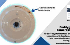
Which embedded antenna to select for a Bluetooth / GNSS application?
Bluetooth, WIFI, ZigBee, ANT, and Wireless Hart – all mentioned radio protocols are using the 2400 MHz band
Even the GNSS band (GPS, Glonass, Galileo, Beidou, QZSS) have to follow the same specifications, because 1575 MHz to 1610 MHz is not far away from the 2400 MHz band. Chip antennas and PCB antennas can be used for GNSS as well. The only what you will miss by using chip and PCB antennas in GNSS applications is the circular polarization. The circular polarisation you get with GNSS patch antennas or helical antennas mainly. In handheld devices is often no space left for an antenna with polarisation. If you open a smart phone, then you will not find a GNSS patch antenna. Even chip antennas are rare to save costs. You will find a bended piece of metal or just a slot in the metal frame.
The chip antennas for GNSS and the 2400 MHz band we can divide in monopoles that has one input for feeding the antennas and loop/PIFA that has a feeding pin and another pin to ground. The PCB track antennas we can divide in monopole and inverted F antenna. There are further options to build a small antenna, but those are not part of this paragraph.
Ceramic loop/PIFA antenna (picture 1)
The ceramic loop/PIFA has a connection on two sides of the antenna. One pin is connected to the transmission line. The other pin is connected to ground. These ceramic chip antennas are often symmetric. It does not matter in which direction it will be mounted on the PCB. Such antennas have regularly a gap with non metal between the antenna and ground plane (on ground chip antennas are rare). This non metal area means non metal on all layers of the PCB. If you have a multi layer PCB, then it makes sense to design the gap on the inner layers a little bit wider. The bottom and the top layer will be used for tuning. The gap can be adjusted by scratching cupper on the bottom and top layer during tuning. With the matching circuit it is possible to tune the antenna as well. If you have a closer look at the data sheet and guide line of the embedded GPS chip antenna, then you will find a length of the reference PCB of 80 mm. The chip antenna is exact in the middle of the 80 mm. If you reduce the 80 mm to 46 mm then you will lose antenna efficiency. The 40 mm to 23 mm left and right of the antenna has to be symmetric. For 2400 MHz applications the standard length is smaller, because the resonant frequency is higher. Please note that you can expect the antenna performance listed in the data sheet only if your design will be close to the reference design. Everything else is a compromise with losing a part of the antenna performance.
Ceramic monopole antenna (picture 2 to 4)
Ceramic monopole antenna you will find at the edges of the PCB. This type of antennas has it need for free space as well. The free space has to be on all PCB layers too. By having a closer look on the dimensions of the antenna in 3D and on the bandwidth you will see that the bigger antennas offer a bigger bandwidth and better performance as well. As bigger the bandwidth is as easier it is to fit in the necessary bandwidth in. At GNSS it the bandwidth is already small, but GNSS is not just GPS anymore. GPS is on 1575.42 MHz and Glonass is up to 1610 MHz. Right now a lot of embedded GNSS antennas cover GPS only. This will change for sure. All new smart phones cover GPS and Glonass. If your device will not support Glonass then the Russian government will charge 25% tax. Combined devices will be taxed with 5% only. Glonass only devices will be not taxed extra.
Back to size and bandwidth: If size does not matter, then select the bigger ceramic antenna. Compare not just the dimensions of the antenna. Have a look on the necessary free space as well. The real space for the embedded antenna is the dimensions of the antenna in 3D plus its free space in 3D.
Ceramic monopole antenna with stub (picture 5)
Most ceramic monopole antennas can be optimized / tuned with a short PCB track on the end of the antenna. Just take care on some free space for the stub on the open end the antenna. With a small PCB track you will the antenna structure a little bit longer. As longer the antenna is, as lower will be the resonant frequency. With such a stub you can reduce the resonant frequency only. If you would like to increase the resonant frequency, then just select another chip antenna from same vendor out of the same antenna family. Be aware that the distance to ground is an option to tune the antenna as well.
PCB monopole antenna – bended monopole (picture 6 and 10)
If you design the PCB monopole antenna at picture 10 right then you get a nearly omnidirectional radiation with loosing of 3 dB antenna efficiency. Sometimes it is better to accept 3 dB loss and to reach an omnidirectional character of the antenna.
PCB inverted F antenna IFA (picture 7 and 9)
If you do not make just a one to one copy, then the inverted F antenna gives you some more options than an embedded monopole. The mentioned rules on distance to ground and free space are related to the IFA as well. There are tons of inverted F antenna shapes listed on Internet. Most of them are copies only and a lot of them are copies of copies. Remember, that even the PCB thickness will effect on the antenna parameters as well.
PCB meandered antenna (picture 8 and 9)
PCB meandered antenna will reduce the mechanical width of the PCB. Meandering of a PCB structure always means a reducing of the bandwidth. As told before any antenna you will select is a compromise often.
Monopole antenna at proximity tag
It is just an example for a bended monopole antenna in a round shape. Be aware that the radius of the antenna shape will affect the antenna performance as well.
Dipole antenna
Dipole antennas are rare in small designs. The reference designs for radio modules / ICs are most time based on monopole antennas. GNSS modules and a lot of other RF modules offer a non symmetric 50 Ohm output to ground. To catch the benefit of dipole antennas you have to invest in a customization.
If you still do not know which antenna type to select for your application, then do not hesitate to drop an email to harald.naumann (at) gsm-modem.de
-
Nothing will interfere your embedded antenna?
-
Why the embedded chip or patch antennas are resonant on the wrong – to high – frequency?
-
How will the ground plane effect your embedded antenna?
-
Which radio approvals has your M2M device to pass?
-
How to connect your embedded antenna with your wireless module?
-
How to design an antenna matching circuit?
-
How to switch between an internal and external cellular or GNSS antenna cheap?
-
Which GPS antenna shall be used for a tracking device?
-
Which embedded antenna to select for a Bluetooth / GNSS application?
-
Dos and don’ts during embedded antenna design in
-
Examples for good and bad M2M designs with embedded antennas
Why the embedded chip or patch antennas are resonant on the wrong – to high – frequency? EA#
Your enclosure will interfere with your embedded antenna
Just have a closer look on some 2400 MHz chip antennas or GPS patch antennas. Some manufacturers offers the embedded antennas with different resonant frequencies. The resonant frequencies are a little bit higher than the frequency you plan to receive.
Why the antennas are resonant on the wrong – to high – frequency?
The answer: As soon you slide your final PCB in your plastic enclosure in the resonant frequency of your antenna will be lower. That means you need embedded antennas that offers in the air (without enclosure) a higher frequency. The jump of the resonant frequency will be interfered by the Epsilon R of the plastic, the thickness of the plastic, and the distance of the plastic to the antenna. Plastic is already the wrong word. Any dielectric material like ABS, glass or acrylic glass will interfere as well. You can´t calculate the jump without a simulation, but you can estimate it if you have experience from former wireless projects. Anyhow, the resonant frequency will jump for sure.
Without experience in RF technology it is highly recommended to hire a third party for consulting. A RF skilled consulter will be able to select the right embedded antenna for your wireless application. Such RF engineers often have access to a huge amount of different antennas. They will be able to optimise the matching circuit between the embedded antenna and the RF generator (e.g. ANT, WIFI, Bluetooth or GSM module) as well.
If you have a need for antenna consulting , then just drop an email to harald.naumann (at) gsm-modem.de
-
Nothing will interfere your embedded antenna?
-
Why the embedded chip or patch antennas are resonant on the wrong – to high – frequency?
-
How will the ground plane effect your embedded antenna?
-
Which radio approvals has your M2M device to pass?
-
How to connect your embedded antenna with your wireless module?
-
How to design an antenna matching circuit?
-
How to switch between an internal and external cellular or GNSS antenna cheap?
-
Which GPS antenna shall be used for a tracking device?
-
Which embedded antenna to select for a Bluetooth / GNSS application?
-
Dos and don’ts during embedded antenna design in
-
Examples for good and bad M2M designs with embedded antennas
Indoor locating – positioning by Bluetooth Low Energy
Indoor locating of a smart phone by Bluetooth Low Energy (e.g. iPhone or Android phone)
Locating of smart phones like an iPhone or Android phone can be done with an app on the device. The app will download the floor plan of the building. Google maps already offers a floor plan generator. Nevertheless such an app will measure the signal strength of RF signals close by. Such signals are transmitted by WIFI routers or the cellular base stations. In public buildings like railway stations or airports you will find a lot of cellular base stations. The coverage goes down to micro cells with a radius of a few meters only. At a rail or at McDonalds you will find a lot of people using their phones. The only option to handle a huge number of phone users staying at the same place is running a micro cell. Anyhow, at such a location you will find a mix of micro cells, mini cells and WIFI routers as well. All this RF signals can be used for a triangulation. But what to do in a town hall, school or museum where you have no cellular cells or WIFI routers indoor? The new Bluetooth specification called Bluetooth Low Energy (BT 4.0, BT Smart) will help to install further RF beacons on low power consumption easy. These Bluetooth Low Energy radio beacons can be used for triangulation as well. The more Bluetooth Low Energy radio beacons you spend the more accurate the result will be. With optimized algorithm and Kalman filters the result can be optimized again. Smart phones of today have more calculation like the server of the indoor locating project at the World Trade Show Expo 2000 in Hannover. The EXPO 2000 was an indoor locating based on GSM cells up and was running. The other great news is that such a Bluetooth Low Energy radio beacon can run on solar or an a standard battery or a mix of both. If you do it right, the Bluetooth Low Energy beacon will run endless.
The further great news is that such Bluetooth Low Energy radio beacons are already in process. I consult the development of the Bluetooth Low Energy radio beacon and can help with the source as well. The project at EXPO 2000 I know very well because I was the project leader. A part of the algorithm was based on my ideas. Today I consult and guideline more than 10 indoor locating / detecting projects in parallel. It is allowed for me to make some of the project step by step public.
If you plan an indoor locating application please do not hesitate to drop an email to harald.naumann (at) gsm-modem.de.
How a good embedded antenna design compromise will look like? EAD#
Embedded chip antenna design example
- Chip antenna mulitband – inverted F antenna
- Type: Inverted F antenna on chip
- Multiband GSM 850 / 900 / 1800 / 1900 / UMTS 2100
- Tuning by matching circuit
- Size of antenna free space: 13.5 mm x 30 mm
- Size of ground plane: 45 mm x 90 mm
- Size of whole PCB: 45 mm x 80 mm (reference design on 45 mm x 114 mm)
This M2M device was planned to be a demonstrator and not for mass production.
Unique features of the M2M device
- Support of USSD instead of SMS and GPRS
- Two layer PCB instead of four layers PCB
- Embedded GSM antenna on small ground plane
USSD is not very common bearer in GSM. A USSD travels from the GSM module to the server and backward estimated one second only. USSD is the fastest bearer in GSM and USSD is the bearer with the lowest power consumption as well.
In the documentation of the manufacturer of the GSM module is a recommendation for a four layers PCB. This design is working well on two layers only. The ground layers of the two layers are connected by vias.
The reference PCB of the GSM /UMTS antenna shows a size of 45 mm x 114 mm. The demonstrator is using a much smaller PCB with the drawback that the antenna efficiency will be minimized.
Do not hesitate to drop an email to harald.naumann (at) gsm-modem.de to get further details of the M2M design. On request you can get the contact details of this project customer as well.
How to switch between an internal and external cellular or GNSS antenna cheap? EA#
M2M devices in cars and trucks have sometimes a need for two antennas. If the external antenna will be demounted or damaged then the M2M device will switch to the internal antennas. Other reason for two antennas could be that the internal antennas on dashboard works fine, but the M2M device will be mounted on a place in a car, where the signal strength is less. The mobile control rooms for police or fire-fighters are a good example for M2M devices in a bus with decreasing the signal field strength by metal roof and metallised windows. Metallised windows we often find in new cars as protection against solar radiation as well.
Be careful by switching the GNSS signal. In year 1999 I ago had to detect where is to front and the back of a heavy machines (20 to 800 meter long) working on railways. Such machines has can work in one direction only. Worst case the machine has to be moved on a long distance to a turntable at railways station. Moving machines on railway costs money. You have to pay per kilometre. The way out was one GPS module with two antennas. The GPS Selective Availability of the US was in this time active. The front and the back were jumping +/- 30 degree on the screen. Railways are long straight lines on a map. Even with the +/- 30 degree fault it was possible to detect the direction of the machine. The only drawback was that the GPS module was completely lost by switching the antenna. It started with downloading the almanac again and made a complete new calculation of the position. If you want two GPS positions in close the same time, then you will run in trouble.
Test your M2M device at laboratory detailed before you move it to the field test.
GaAS switch
If you search on Google for GaAS switch, then you will find a lot of examples for such RF switches.
By selection of the GaAS switch just take care on
- Frequency range cellular (e.g. LTE 698, 800, 2100, 3500 MHz GSM EU 900 and 1800 MHz)
- Frequency range GNSS (GPS 1575,42 MHz and Glonass up to 1610 MHz)
- Maximum current (GSM transmits in peaks with 2 Ampere, this will force TX power peaks as well)
- Low insertion loss
- Low harmonic distortion
- Good isolation
If you are still not sure which RF switch to select then just drop an email to harald.naumann (at) gsm-modem.de
-
Nothing will interfere your embedded antenna?
-
Why the embedded chip or patch antennas are resonant on the wrong – to high – frequency?
-
How will the ground plane effect your embedded antenna?
-
Which radio approvals has your M2M device to pass?
-
How to connect your embedded antenna with your wireless module?
-
How to design an antenna matching circuit?
-
How to switch between an internal and external cellular or GNSS antenna cheap?
-
Which GPS antenna shall be used for a tracking device?
-
Which embedded antenna to select for a Bluetooth / GNSS application?
-
Dos and don’ts during embedded antenna design in
-
Examples for good and bad M2M designs with embedded antennas
How a wrong embedded antenna design could look like? EAD#
Embedded antenna design mistakes
- Type: Meander with spiral
- Multiband (or GSM 900 / 1800 or GSM 850 / 1900)
- Not easy to tune on center frequency because the 900 MHz part goes straight to the 1800 MHz part
- Not easy to tune on antenna impedance
The GSM antenna structure at the picture is a shape that normally is in use with PCB antennas and coaxial cable. Such antenna structures are optimized on 4 to 8 cm distance to ground plane. A further design mistake is the ground area left and right of the antenna. Radio waves are travelling like light. The antenna is the “candlelight”. The ground area left and right will build shadows for the radio wave. The antenna structure is to close to ground plane and the connector is to close to the embedded antenna as well. Worst case the embedded GSM antenna will interfere with the GSM module. The GSM 900 part on the border of the PCB is very close to the plastic enclosure as well. The to close plstic enclosure will generate a parasitic load again. The blue marked area shows the “visible” ground plane of the antenna. Embedded GSM antennas like GSM chip antennas or embedded GSM PCB antennas are looking for 40 mm to 90 mm up to 40 mm to 110 mm ground plane. The blue aera has a size of estimated 40 mm x 30 mm.
Embedded GSM antenna on minimized ground plane
Read more: How will the ground plane effect your embedded antenna?
How to optimize this embedded GSM antenna design?
Start with reading here:
Nothing will interfere your embedded antenna?
And read all linked chapters!
GSM PCB antenna recommendations based on the picture
- Remove the embedded GSM antenna on small side of the PCB
- PCB size 40 / 50 mm x 90 to 110 mm
- Antenna needs bigger distance to ground plane
- No ground areas left and right of the antenna
- No parasitic load by plastic enclosure close to the antenna
- No parasitic load by the metal screws of the enclosure
- No cut and paste of an antenna structure
Not checked (details missed)
- Impedance of transmission line
- Number of PCB layers
- Number of vias
- Size of real ground plane area based on Gerber files
- Ground pins of GSM module to ground plane
- PCB tracks for supply voltage to GSM module
- Capacitors to block the GSM peak current
- Power supply to support the GSM module
- Place of the SIM card holder
- Capacitors close to SIM card holder
- Everything related to GPS
- Everything related to emission
- Everything related to radio approvals like R&TTE
This embedded design example has reach us, after finishing the first PCB. It is better to go the other way around. In the first step you tell the size and material of the enclosure. In second step a RF consulter will make a proposal for the antenna. The best and cheapest result you get, if you select the embedded antenna first and design the product around. Even better is, to give the freedom on a resonable size for a ground plane.
If you still not sure which antenna to select and why, then do not hesitate to drop an email to harald.naumann (at) gsm-modem.de
Which GPS antenna shall be used for a tracking device? EA#
The sketch about GPS antennas was made during a training about wireless
1. GPS chip antenna as PIFA
One option are GPS PIFAs. Such PIF antennas are looking for 70 to 80 mm long PCBs. 35 to 40 mm left and 35 to 40 mm right is fine. The shorter the PCB length, the worst the antenna efficiency will be. With 22.5 mm left and 22.5 mm right, you still get a nice result. The length in direction X has to be at least 45 mm. In Y direction the size does not matter.
The centre frequency of this PIFA antenna can be tuned with the gap (ground less area) under the antenna plus matching circuit.
2. – 4. GPS chip antennas as monopole antenna
Option 2 and 3 are showing antennas on the corner of the PCB. Just take care on the data sheets of the GPS antennas. The distance to ground plane is maybe different, by several types of antennas. This antenna type can be tuned by making a stubby (small PCB track) on the open end of the antenna and components in the matching circuit.
5. GPS patch antenna on PCB
Most data sheets name a 70 x 70 mm or 35 x 35 mm ground plane. If you change the size of the ground plane, then the centre frequency will shift. If you put an enclosure on top of the antenna, then the centre frequency will shift again. If you change the thickness of the plastic or the type of the plastic or the distance to the plastic – every change will interfere with the antenna.
5.1 The way out of the GPS patch antenna jungle
Just ask for an evaluation with GPS patch antennas, that comes with centre frequencies of 2 MHz steps. One out of 10 antennas will fit to your application. To limit the tuning trouble you shall select a 25×25x4 mm GPS patch antenna. As bigger the GPS patch antenna is, as bigger the bandwidth of the antenna. As bigger the bandwidth, as less the risk to loose performance. A GPS patch with a size of 18×18x4mm is a good compromise.
6. – 7. GPS patch antenna on non symmetric PCB
GPS patch antennas offers a circular polarisation. The circular polarisation you get by putting the feeding point not in the middle of the GPS patch antennas. The red round shaped lines on the sketch number 6 shows the floating current on your PCB. The current will float circular. Sketch number 6 shows a 40×40 mm PCB. This is OK. At sketch number 7 you see a non symmetric PCB. As soon, the PCB is not quadratic the circular polarisation will be destroyed and the loss will be 3 dB. If your PCB is not quadratic (what is common) then just take care, that the ground plane will be quadratic.
Further GPS antenna types
GPS is on 1575.42 MHz. In this frequency range you can use PCB track antennas inside PCB as well. Such PCB tracks will like the GPS chip antennas have no circular polarisation. Other types are helical antennas on top of the enclosure. Helical antennas you can get unbalanced or balanced with balun. There are helical antennas with SMT mounting as well. Another option are active GPS antenas with short coaxial cables or active GPS antennas to be mounted direct on the PCB.
Conclusion
The selection of the GPS antenna and the tuning plus selection of the GPS module is a difficult task.
If you still not sure which GPS antenna to select and why, then do not hesitate to drop an email to harald.naumann (at) gsm-modem.de
-
Nothing will interfere your embedded antenna?
-
Why the embedded chip or patch antennas are resonant on the wrong – to high – frequency?
-
How will the ground plane effect your embedded antenna?
-
Which radio approvals has your M2M device to pass?
-
How to connect your embedded antenna with your wireless module?
-
How to design an antenna matching circuit?
-
How to switch between an internal and external cellular or GNSS antenna cheap?
-
Which GPS antenna shall be used for a tracking device?
-
Which embedded antenna to select for a Bluetooth / GNSS application?
-
Dos and don’ts during embedded antenna design in
-
Examples for good and bad M2M designs with embedded antennas
How a good embedded antenna design will look like? EAD#
Embedded antenna design examples
- PCB antenna dualband – inverted F antenna
- Type: Inverted F antenna
- Multiband (e.g. GSM 900 / 1800 or GSM 850 / 1900)
- Easy to tune on center frequency
- Easy to tune on antenna impedance
- Size of antenna structure: 50mm x 10 mm
- Size of ground plane: 50 mm x 90 mm
- Size of whole PCB: 50 mm x 100 mm
This M2M device was designed by following all important rules of embedded antenna design. The developer got advice by an engineer with skills in antennas and long time experience in development of M2M devices. In this M2M design, the embedded PCB antenna was selected first. The ground plane length was selected by the lowest to frequency to transceive. If you have a closer look, then you will see that there are no holes for screws in the corners of the device. The screw that will be close to the radiator for GSM 850 / 950 will be made in plastic. This will help to minimise the parasitic load to the antenna. Between the GSM module and the embedded PCB antenna is a semiconductor that works as a 50 Ohm switch to an external antenna. The first quick performance test was done by the embedded channel scanner of the GSM module. The scanning of all GSM base station with external magnetic mount GSM antenna on big metal plate parallel to the embedded PCB antenna has shown, that the embedded GSM antenna catch more GSM base stations then magnetic mount antennas. The M2M device is in use in inside vending machines. Even inside the vending machines the signal strength is high enough to save the USD 4 for the external magnetic mount antenna, the drilling of holes at vending machines and the manual work for mounting antenna and coaxial cables. This saves further USD 8. All together the solution saves USD 12 per installation. The size of the first project is 4000 vending machines. This project customer will save USD 12 x 4000 = USD 48.000 with the first vending project.
Do not hesitate to drop an email to harald.naumann (at) gsm-modem.de to get advice on how to design a M2M device. On request you can get the contact details of this project customer as well.
How to design an antenna matching circuit? EA#
Antenna impedance matching is an important part of any M2M design.
The input impedance of an antenna needs to be close to the impedance of the radio module. If not then the signal will be reflected back to the radio module. The signal will not be radiated by the antenna. Matching circuits often contains several discrete inductors and capacitors. Even transmission lines can be used to convert the impedance between radio module and antenna.
Matching 50 Ohm impedance
Radio modules (e.g. GSM, HSPA, LTA, Bluetooth, WIFI or GPS) mostly come with a balanced output of 50 Ohm. The impedance of the selected chip antenna or PCB antenna can differ. Often the center frequency or impedance of the antenna jumps a little bit by thickness of PCB or distance to housing or thickness of the housing. All this can be adjusted by matching circuit. Be aware, that the matching circuit will add a loss or will reduce the bandwidth of the selected antenna. The better option is to tune the antenna itself by changing the antenna structure. By using chip antennas out of the shelf you can´t touch the structure. Nevertheless the gap between antenna and ground plane can be used for matching as well. In an ideal world the matching circuit will adjust the output impedance of the radio module to the antenna input impedance. This will end in higher TX power output of the antenna and the optimise RX sensitivity as well.
Balun between radio module and antenna
Radio modules (e.g. GSM, HSPA, LTA, Bluetooth, WIFI or GPS) often come with balun inside. The matching network for designs on chip level acts as the balun transforming the balanced output of the integrated circuit to the unbalanced antenna. Using of radio modules with internal balun force you to select monopole antennas. In some cases balanced output to dipole antennas gives you a benefit, because e.g. a dipole offers a higher antenna gain.
DC blocking
Inside of the balun is often a capacitor. The capacitor blocks the DC voltage from antenna. By GPS modules with active GPS antennas this is inverse. You need the DC voltage at the antenna. Some GPS modules have a DC switch inside, some other shows a DC coupling outside of the GPS module. Just follow the specification of the reference design of the manufacturer.
Harmonic suppression
By chip designs the balun rejects harmonics and out of band emissions. The maximum band emissions are specified e.g. at FCC or R&TEE.
Examples for antenna matching circuits
In first step you follow the specification of the supplier of your embedded antenna. If if it not clear then just replace the capacitor in row to a zero Ohm resistor. Worst case the antenna will be mismatched, but will radiate something. For your first steps and tests this is fair enough. Be aware that a big reflected wave can puzzle your radio modules or will generate emissions on your PCB. The final matching circuit cut be just one capacitor or inductor in row (picture 1). You also could end with a Pi circuit (picture 2 and 3). Take care on enough place for components close to the antenna and select capacitors and inductors with small footprint, because smaller footprints will help with less parasitic effects. Each capacitor contains an inductive part and each inductor has a capacitive part as well. Never change the manufacturer of the components you selected during the antenna matching circuit. Take care that the Epsilon R of your FR4 is always the same in each production lot. Best is not the change the supplier of the manufacturer of the PCBs as well. Be aware that impedance testing of your PCB makes the production more expensive and to not save the money for impedance testing of your PCBs.
If you are still not sure how to design the antenna matching circuits just ask for advice by a third party with skills in radio technology and using a network analyzer. Plan one to three working days for optimization the antenna matching. The antenna matching has to be done with final enclosure, because the Epsilon R of your plastic and the thickness of the plastic will effect to the antenna as well.
-
Nothing will interfere your embedded antenna?
-
Why the embedded chip or patch antennas are resonant on the wrong – to high – frequency?
-
How will the ground plane effect your embedded antenna?
-
Which radio approvals has your M2M device to pass?
-
How to connect your embedded antenna with your wireless module?
-
How to design an antenna matching circuit?
-
How to switch between an internal and external cellular or GNSS antenna cheap?
-
Which GPS antenna shall be used for a tracking device?
-
Which embedded antenna to select for a Bluetooth / GNSS application?
-
Dos and don’ts during embedded antenna design in
-
Examples for good and bad M2M designs with embedded antennas
Dos and don’ts during embedded antenna design in EA#
The list is not complete. It should just help to avoid the basic mistakes that other developers with no or less RF skills have done before.
- Take care on a reasonable ground plane for the monopole antenna and remember that the size of the ground plane is related to the lowest radio frequency that the M2M device have to transceive
- Remember the tips and tricks you can use to make the ground plane bigger
- Select your embedded antenna carefully and have a closer look on the antenna efficiency special at the lower frequencies that the M2M device has to transmit and to receive (e.g. GSM 850 = 824 MHz or LTE 700 = 698 MHz)
- If you plan to enter non local markets like USA, China, Brazil or China then have a closer look on national regulations and specifications (e.g. RSE, TRP, TIS). Remember that R&TTE is an easy task because it requests no TRP and TIS like the operator approval of AT&T
- Remember that an external stubby helical antenna is most time a monopole antenna with a need for ground plane
- Remember that PCB antennas with coaxial cables are often planned to be mounted at least 20 mm far away from the ground plane and metal layer
- Do not place the ground layer, the supply voltage layer or any other PCB layer underneath the embedded antenna (e.g. chip antenna)
- Do not place traces underneath the antenna
- Do not place the antenna very close to metallic objects (e.g. screws of the enclosure, battery, display, shielding and buttons)
- Do not place the antenna too close to dielectric materials like plastic enclosures, plastic screws, keypads or acrylic glass
- Do not expect to reach the antenna parameter (gain, antenna efficiency, radiation pattern) listed in the data sheet and measured on an evaluation board without spending time and effort on tuning
- Do not tune the embedded antenna in free air and remember that different kind and thickness of plastic will have an effect on the embedded antenna
- Take care that the enclosure is non metal and that the plastic does not contain metal or carbon
- If possible test the selected plastic for high RF losses before field tests and mass production
- Never make a one-to-one copy of an antenna design and expect it to work without testing and tuning
- Do not use too thin PCB tracks or too long PCB tracks to minimize the loss between transceiver and antenna and replace the PCB tracks to a coaxial cables if the distance between antenna and transceiver will be too long
- Remember that the final design is always a compromise and that you often will not reach the same result like tested on reference PCB
- If the RF skills of your own developer team are too low, hire an external consulter
If you have hints and tips that should be listed in the upper list then just drop an email to harald.naumann (at) gsm-modem.de. Any feedback by comment id is welcome as well.
-
Nothing will interfere your embedded antenna?
-
Why the embedded chip or patch antennas are resonant on the wrong – to high – frequency?
-
How will the ground plane effect your embedded antenna?
-
Which radio approvals has your M2M device to pass?
-
How to connect your embedded antenna with your wireless module?
-
How to design an antenna matching circuit?
-
How to switch between an internal and external cellular or GNSS antenna cheap?
-
Which GPS antenna shall be used for a tracking device?
-
Which embedded antenna to select for a Bluetooth / GNSS application?
-
Dos and don’ts during embedded antenna design in
-
Examples for good and bad M2M designs with embedded antennas
.
Email to Harald
Harald@Facebook
Harald@Google+
Harald@Linkedin
Harald´s website
M2M on Twitter
Posts by RSS


