There is no reference for antennas on extremely small boards in small packages. Cellular chip antennas of different manufacturers all have a reference ground plane of approx. 45 mm +/- 10 mm x 100 mm +/- 20 mm. Nobody can cheat the physics. The length of the PCB influences the return loss. This is documented in my IoT / M2M Cookbook. In the Cookbook the same antenna was measured on different PCBs.
NB-IoT chip antenna
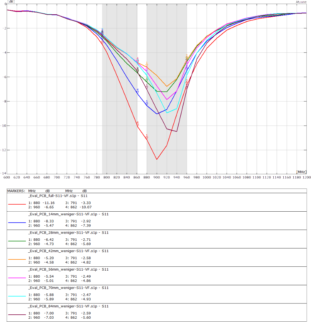
NB-IoT chip antenna , return loss
The NB-IoT chip antenna has a reference ground plane of 35 mm x 115 mm. The red curve is showing the return loss on the full length of the PCB. All other curves show what happens if you shorten the PCB by 14, 28, 42, 56, 70 and 84 mm. The center frequency of the NB-IoT antenna shifts upwards. At the cyan curve it gets even better again. The edge length of the PCB also has a strong influence on the resonance frequency.
If you take a second look at the return loss, you can see that the NB-IoT chip antenna does not cover band 8 and band 20 in total. Wrong return loss will lead to harmonic harmonics. The IoT device will then fail the radio tests in the test laboratory.
If you have your own customized NB-IoT antenna then you can adjust the center frequency of the antenna by the length of the radiator. This is not possible with NB-IoT chip antennas.
With a smaller PCB the effort in antenna development increases. Chip antennas often fail. The minimum size of an antenna was discovered by Lan Jen Chu between 1948 and 1960. His theses were then optimized again, but the basic statement of Chu has not changed. In electrical engineering Chu limit for a small radio antenna. In practice this means that there is a limit to the bandwidth of data that can be sent to and received from small antennas such as are used in mobile phones.
PCBs which differ from the size 45 mm +/- 10 mm x 100 mm +/- 20 mm lead to additional effort when integrating the antenna. The same applies to round or curved surfaces. The antenna is not only the component we see but the component (antenna) with the board and the housing. Antennas are also not components but systems.
If you want to know exactly, you can copy the well documented GSM antenna in my book and make changes. This requires a VNA, a lot of time and experience. Only through practice and measurement setups can you learn which changes have an effect. Once the required return loss has been achieved, the radiation pattern must also be checked.
We are happy to take all the worries away from the developers. In the first step, we develop empty circuit boards with chip antennas, flex PCB antennas, helical antennas and many other types and measure them in the housing. If large metallic surfaces, such as display or battery, are in the neighborhood, they are also included in the PoC. With customer-specific antennas, the process is the same. The result will be handed over to the customer and the customer will integrate it into his PCB with all components with housing. At the end, the entire device is measured again with the VNA.
If you want to get rid of your worries please send an email to harald.naumann (at) lte-modem.com.