Paring by NFC/RFID for any M2M device – a dream comes true
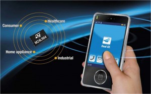
With this new NFC/RFID on chip all NFC/RFID enabled devices like smart phones or tablets or RFID readers can read and write to the chip. The chip is a NFC/RID tag on ISO/IEC 15693 that you just solder on your PCB. The NFC/RFID antenna could be a PCB track, a SMT mounted coil antenna, a structure made by laser on your plastic enclosure or a customized wire loop antenna. About NFC/RFID antennas on 13.56 MHz we will tell more in another story later.
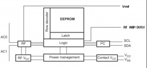
The chip does not just contain the NFC/RFID transceiver – it contains an EEProm as well. The EEProm (4 KB, 16 KB or 64 KB) can be by accessed by NFC/RFID or wired bus (I2C). You can select which memory banks can be written by radio or I2C or both communication channels. Based on the two communication channels you can pair your WIFI, Classic Bluetooth, Bluetooth Low Energy, ANT+ or any other wireless link easy. Nevertheless, the EEProm can be used for setting parameters like communication language in the display of your M2M device easy as well. You can set the parameters without opening the enclosure. This is e.g. a very helpful feature for IP65 or IP67 protected M2M devices, but helps to save time for screwing or helps to save a USB connector at your enclosure.
There is not just the NFC/RFID on chip available
You can get ready to use NFC/RFID readers/writers, reference designs for own NFC/RFIF readers/writers, cheap smart phones like the Samsung S3 mini or several Android tablets. List of NFC phones is published here http://www.tagonic.com/supported-devices . Last but not least the chip offers an energy harvester. One pin can be used to drive or charge your M2M device. It also can be used for wake up on NFC/RFID radio as well.
The NFC/RFID on chip is available with an evaluation kit that contains the chip wired on a PCB including an 8 bit microcontroller, a temperature sensor or a display and the NFC/RFID antenna. The same evaluation kit contains an NFC/RFID reader/writer as well. Both PCBs are very well documented and ready to copy and redesign. For Android phones a free of charge app is available. That means you can use the reader/writer with demo software on your Windows PC or the Android phone to access the chip.
Kit for evaluation of the NFC on chip
The kit for evaluation contains the M24LR04E-R Dual Interface EEPROM IC. This kit contains 2 different boards:
1) The M24LR board is battery-less and powered by RFID readers or NFC-enabled phones supporting ISO/IEC 15693.
2) The RF transceiver board is an RFID reader demonstration board and is composed, among other parts, of a CR95HF (13.56 MHz multi-protocol contactless transceiver IC with SPI and UART serial access). This board has to be plugged in to a PC and comes with demonstration software.
The M24LR board also works with Android NFC phones supporting ISO/IEC 15693. An application called NfcV-Reader is available on Google Play. Performance may vary depending on NFC phone’s RF management.
Key features of the NFC/RFID on chip
- Radio interface
- ISO 15693 and ISO 18000-3 mode 1 compatible
- 13.56 MHz ±7k Hz carrier frequency
- To tag: 10% or 100% ASK modulation using 1/4 (26 Kbit/s) or 1/256 (1.6 Kbit/s) pulse position coding
- From tag: load modulation using Manchester coding with 423 kHz and 484 kHz subcarriers in low (6.6 kbit/s) or high (26 kbit/s) data rate mode. Supports the 53 kbit/s data rate with Fast commands
- Internal tuning capacitance: 27.5pF
- 64-bit unique identifier (UID)
- Read Block & Write (32-bit blocks)
- Wired I2C interface
- Two-wire I2C serial interface supports 400 kHz protocol
- Single supply voltage:
- 1.8 V to 5.5 V
- Byte and Page Write (up to 4 bytes)
- Random and Sequential read modes
- Self-timed programming cycle
- Automatic address incrementing
- Enhanced ESD/latch-up protection
- I²C timeout
- Digital output pin
- User configurable pin: RF write in progress or RF busy mode
- Energy harvesting
- Analog pin for energy harvesting
- 4 sink current configurable ranges
- Memory
- 16-Kbit EEPROM organized into:
- 2048 bytes in I2C mode
- 512 blocks of 32 bits in RF mode
- Write time
- I2C: 5 ms (max.)
- RF: 5.75 ms including the internal Verify time
- More than 1 million write cycles
- More than 40-year data retention
- Multiple password protection in RF mode
- Single password protection in I2C mode
- Package
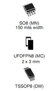
- ECOPACK2®(RoHS compliant and Halogen-free)
- 16-Kbit EEPROM organized into:
If you want for more details about this NFC/RFID chip, a free of charge webinar, a study, a research, a prototype or a development of a wireless M2M product then just send an email to harald.naumann (at) gsm-modem.de


