The simulation is taken from my IoT / M2M Cookbook. About 30 % of the book is about the integration of antennas into an enclosure. The antenna structure is explained in detail in the book and can be easily reproduced.
GSM PCB antenna simulation
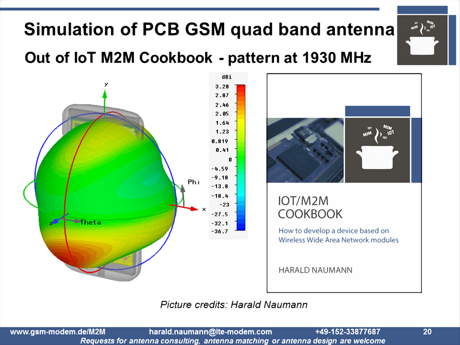
The green to yellow marked area shows the radiated power from 0 dBi to 1.64 dBi. The peak of the radiated power is 3.28 dBi. Since the antenna gain is given in the main beam direction, the data sheet would then show 3.28 dBi. In the truthful data sheet, the average antenna gain would be about 1 dBi. Please note that the losses in the housing are already included in the simulation. Datasheets for chip antennas always contain the data without the losses in the enclosure. The antenna structure is located at the upper end of the PCB. The highest radiation can be found in the lower quarter of the board. It is not the antenna that radiates the energy, but the whole PCB. The antenna generates turbulence currents on the PCB and these currents then generate the electric and magnetic fields. The radiator, which we call the antenna, and the PCB form the antenna. The influence of the printed circuit board and the influence of the enclosure is explained in the following slides.
If you are planning an IoT device with an integrated antenna, your requests for suggestions are welcome. If your design is already finished, we are happy to do the matching for you. If you have problems with radio certification or no room for a chip antenna, we will be happy to develop a customer-specific antenna. If you are using a chip antenna and want to reduce costs, we will be happy to develop an antenna with a BOM of 0 USD in the main board for you. Please contact harald.naumann (at) lte-modem.com for more information.