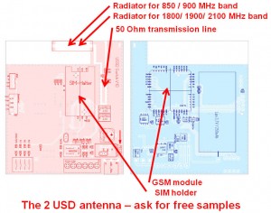
Embedded chip antenna design example
- Chip antenna mulitband – inverted F antenna
- Type: Inverted F antenna on chip
- Multiband GSM 850 / 900 / 1800 / 1900 / UMTS 2100
- Tuning by matching circuit
- Size of antenna free space: 13.5 mm x 30 mm
- Size of whole PCB: 45 mm x 80 mm (reference design on 45 mm x 114 mm)
This M2M device was planned to be a demonstrator and not for mass production.
Unique features of the M2M device
- Support of USSD instead of SMS and GPRS
- Two layer PCB instead of four layers PCB
- Embedded GSM antenna on small ground plane
USSD is not very common bearer in GSM. A USSD travels from the GSM module to the server and backward estimated one second only. USSD is the fastest bearer in GSM and USSD is the bearer with the lowest power consumption as well.
In the documentation of the manufacturer of the GSM module is a recommendation for a four layers PCB. This design is working well on two layers only. The ground layers of the two layers are connected by vias. With connecting the ground layers you do not double the ground plane. If you use two layers only, then these two layers will hold all components and the PCB tracks as well. That means you will have an inhomogeneous areas with ground on both layers and the target is to get a nearly homogeny ground area by connecting top and button layer together.
The reference PCB of the GSM /UMTS antenna shows a size of 45 mm x 114 mm. The demonstrator is using a much smaller PCB with the drawback that the antenna efficiency will be minimized.
Do not hesitate to drop an email to harald.naumann (at) gsm-modem.de to get further details of the M2M design. On request you can get the contact details of this project customer as well.
